Migrating analog IP to a new foundry or process node is never a simple “shrink and go” exercise—especially when high-frequency (HF) design is involved. At RF and multi-GHz speeds, even small changes in parasitics, device models and substrate behavior can derail performance. For engineering teams exploring migration, understanding these HF-specific risks is essential to avoid surprises in silicon.
What makes HF migration different?
At high frequencies, analog and RF performance hinges on small-signal behavior, which is highly sensitive to parasitic elements and layout-dependent effects. Two key metrics—fT (intrinsic speed) and fMAX (power gain limit)—must be re-validated after migration. While fT may remain stable, fMAX often shifts due to changes in gate resistance, overlaps and substrate paths.
This sensitivity means that even DRC-clean layouts can behave differently post-migration. Advanced modeling flows that account for layout-dependent effects (LDE) and variability are critical to predicting how “as-manufactured” designs will perform.
Modeling and measurement: The real migration challenge
Successful HF migration is fundamentally a modeling and measurement problem. Engineers must go beyond basic checks and re-characterize several aspects of their design:
- Gate resistance (RG): Impacts input impedance, noise figure and fMAX. Migration requires accurate RG extraction using the target PDK’s models.
- Non-quasi-static (NQS) effects: These become significant at high speeds and must be enabled in compact models’ post-migration.
- Bias-dependent capacitances: Overlap and fringing capacitances shift with bias and geometry.
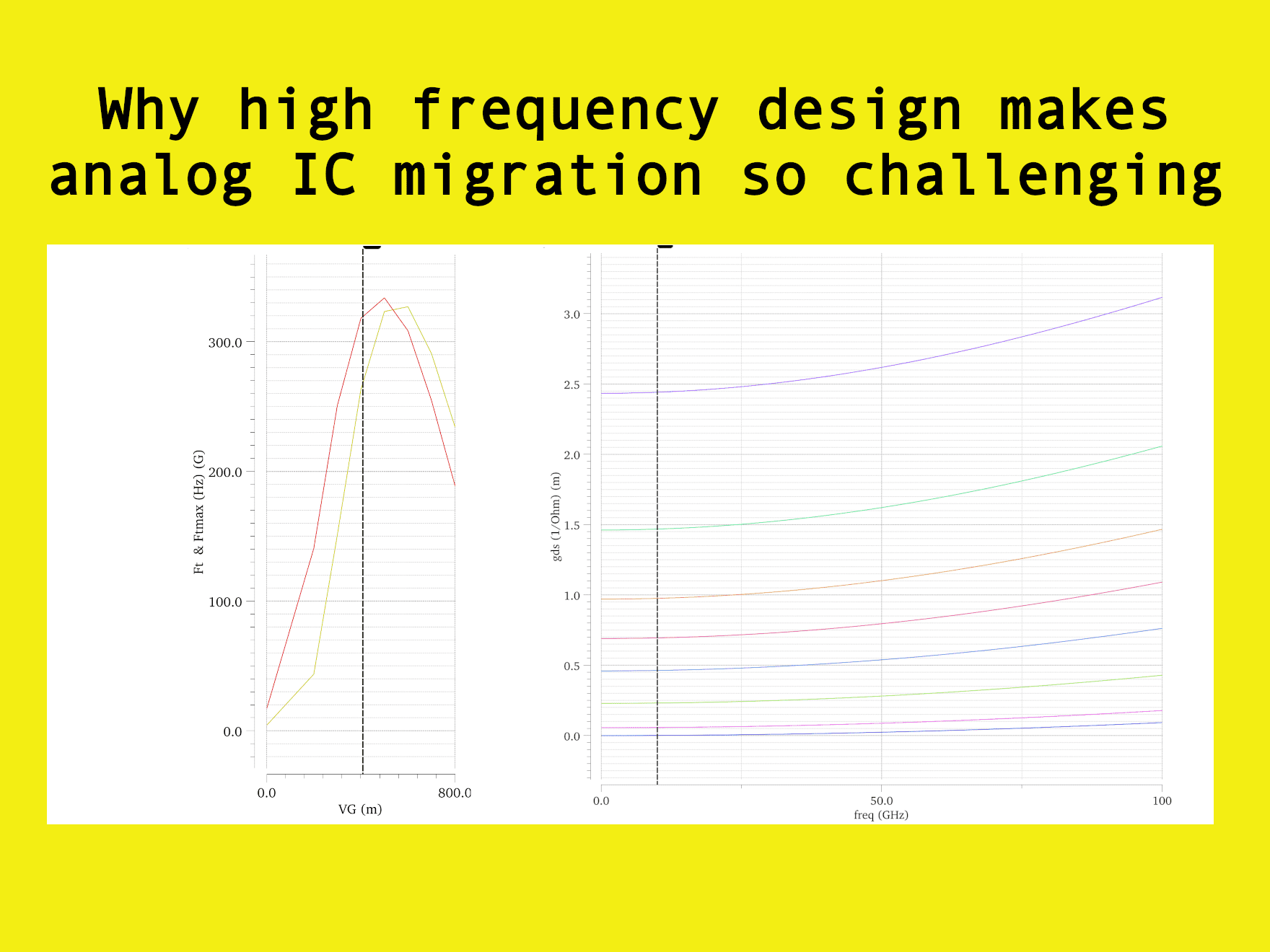
Figure 1 and Figure 2 illustrate example analysis plots. The first for fT / fMAX and Gate Resistance RG versus gate voltage and the second GDS (Drain-Source Conductance) and Cgs (Gate-to-Source Capacitance) versus frequency.


Interconnect and passive components: Hidden pitfalls
At GHz frequencies, interconnect resistance and inductance increase due to skin and proximity effects. Migration demands frequency-aware RLC extraction—not just RC models. Differences in metal stack thickness and sheet resistance across PDKs can alter bandwidth and matching.
Passive components also require re-qualification:
- Metal-Insulator-Metal (MIM) capacitors: Equivalent Series Resistance (ESR) increases with frequency due to the skin effect and is the vital parameter for assessing the Qualify Factor (Q) of the MIM capacitor. Wide band models are essential to evaluate and maintain Q across operating frequency.
- On-chip inductors: Losses from eddy currents and substrate coupling vary with resistivity and metal thickness. Model refitting is essential and can be guided by S-parameter analysis which helps define key fitting parameters.
Substrate and technology differences
Substrate resistivity and well structures affect RF isolation and thermal behavior. Moving between bulk CMOS and FDSOI introduces differences in body biasing and self-heating, which must be modeled and verified.
Measurement correlation and thermal effects
S-parameter de-embedding must be re-established to ensure accurate gain and noise predictions. Pad stack variations can mislead results if not properly accounted for.
Self-heating and EM/IR effects also become more pronounced at advanced nodes. These influence transconductance and noise, requiring thermal-aware simulation and verification.
Within an an analog IC migration, adjustments to metal tracks sizes may be required to support original current density criteria. That is mainly a DC / low frequency concern and the topic is addressed in our blog posting “The Hidden Threat in Analog IC Migration: Why Electromigration rules can make or break your next tapeout“.
A practical HF migration checklist
To ensure first-pass success, Thalia recommends a 7-step checklist:
- Re-characterize fT and fMAX
- Confirm compact model options (NQS, RG)
- Use frequency-aware RLC extraction for interconnects
- Re-fit passive models (MIM, inductors)
- Re-assess substrate coupling and isolation
- Re-establish S-parameter measurement correlation
- Enable self-heating and EM/IR co-analysis
{Thalia’s AMALIA platform does not address heating, EM/IR analysis.}
Final thoughts
Analog IP migration at high frequencies isn’t a black art—but it’s not a push-button task either. It’s a constraint-preserving rebuild followed by physics-aware optimization. With the right modeling, measurement and verification practices, teams can migrate confidently and predictably.
Thalia’s AMALIA platform supports this journey with automation for pattern recognition, device stretching and layout preservation—integrating seamlessly with Cadence® design flow and Siemens EDA’s Analog FastSPICE™. If you’re exploring migration, we’d be happy to share real-world case studies and actionable checklists.
Trademark acknowledgment
Cadence and Analog FastSPICE are marks of Cadence Design Systems and Siemens Industry Software Inc respectively.
Use of these names and other companies and products does not imply endorsement.