Thalia and X-FAB Forge Strategic Partnership to Safeguard Supply and Accelerate IP Migration

Cwmbran, United Kingdom – 23rd September 2025 – Thalia Design Automation, a leader in analog, mixed-signal and RF IP migration solutions, today announced a strategic partnership with X-FAB, the world’s leading analog/mixed-signal specialty foundry.
The partnership will provide X-FAB customers with advanced migration capabilities to transition designs quickly and cost‑effectively to long‑term, secure process technologies.

The partnership addresses critical market challenges including end-of-life process technologies and supply chain security, where semiconductor companies must rapidly migrate existing designs to ensure continuity of supply.  As customers seek greater flexibility and resilience in their supply chains, the combined expertise of Thalia and X-FAB ensures a seamless design transfer.  This is critical to protect product lifecycles, maintain market commitments and minimize business disruption.

The agreement provides Thalia with access to X-FAB’s Process Design Kits (PDKs), enabling its AI-powered AMALIA Platform to be optimized for X-FAB’s specialist process portfolio.  This delivers migration outcomes precisely tuned to X-FAB’s technologies, preserving design integrity and meeting demanding performance and qualification requirements.

“By integrating Thalia’s migration technology into our ecosystem, we are offering customers a proven method to prolong their revenue streams even in case of unavoidable process changes,” said Damien Macq, COO at X-FAB.  “This partnership aims to enhance customer confidence, secure long-term supply and support the use of our specialty technologies throughout their full products’ lifecycle.  It demonstrates how we assist customers in maintaining competitiveness in changing market conditions.”

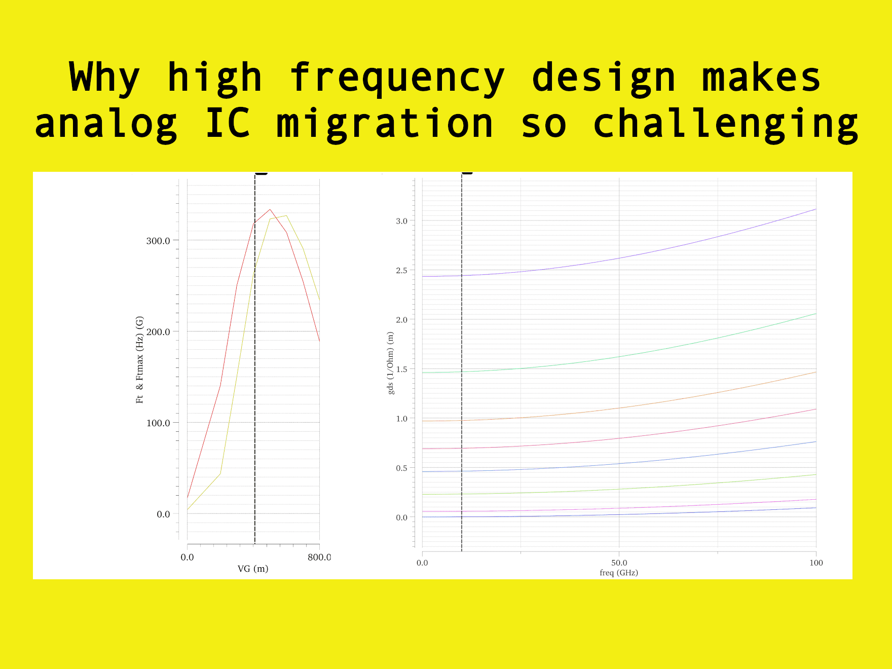
For X-FAB customers, the AMALIA Platform significantly reduces the complexity and cost of migrating existing designs while preserving critical performance metrics.  Automated layout porting and optimization, combined with silicon-proven validation, enable faster time-to-market compared to traditional manual redesign methods.

“We’re excited to bring our migration expertise to X-FAB’s global customer base,” said Sowmyan Rajagopalan, CEO of Thalia. “By combining our AI-driven automation with X-FAB’s world-class manufacturing capabilities, we are enabling customers to respond quickly to market or supply changes while unlocking the benefits of X-FAB’s unique specialty processes.”

About X-FAB

X-FAB is a global foundry group providing a comprehensive set of specialty technologies and design IP to enable its customers to develop world-leading semiconductor products that are manufactured at X-FAB’s six wafer fabs located in Malaysia, Germany, France, and the United States.  With its expertise in analog/mixed-signal technologies, microsystems/MEMS, Photonics, silicon carbide (SiC) and gallium nitride (GaN), X-FAB is the development and manufacturing partner for its customers, primarily serving the automotive, industrial and medical end markets.  X-FAB has approximately 4,500 employees and has been listed on Euronext Paris since April 2017 (XFAB). For more information, please visit www.xfab.com.

About Thalia Design Automation

Thalia is a leading provider of analog, mixed-signal and RF IP design migration solutions. The company’s AMALIA Platform harnesses advanced automation and AI/ML technology to streamline the migration process, enabling semiconductor companies to reduce time, cost and complexity while optimizing their ability to create innovative applications. Thalia serves customers worldwide across automotive, communications, consumer electronics and industrial markets. For more information, visit thalia-da.com.

Press contacts

Why Callbacks Break Automated Analog IC Migration Tools — And What You Can Do About It

If you’re a senior analog IC designer, you’ve likely heard the pitch: “Automated migration tools can seamlessly port your designs to new process nodes.”  But when it comes to real-world analog design, that promise often falls short. One of the biggest reasons? Callbacks.

In this post, we’ll unpick why callbacks are a hidden obstacle in analog design migration—and why most automation tools struggle to handle them effectively.

What are callbacks in analog IC design?

Callbacks are custom scripts or functions embedded in your design environment.  They’re triggered by specific events—like a layout change or a parameter update—and they automate tasks such as:

  • Validating custom design rules
  • Modifying device parameters based on process-specific behavior
  • Adjusting device dimensions based on layout geometry
  • Enforcing matching conditions in differential pairs

They’re powerful.  They’re flexible.  And they’re deeply tied to your current process node.

Why callbacks are a migration headache

Callbacks in a new PDK can be considered unpredictable.  They can have tool dependency and version sensitivity.  They may lack documentation and transparency.  The PDK specific rules which callbacks enforce can conflict with legcy design intent.  And in the complex world of design migration changes causes by callbacks can break analog matching, introduce parasitics or violate design intent.  In short,  they abide by strict rules.

When migrating analog designs to a new process node—say, from 40nm to 22m—callbacks become a liability.  Here’s why:

1. Process-specific logic that doesn’t translate

Callbacks are often written with hard-coded assumptions about the original process node. These include:

  • Calculation of layout-dependent parameters
  • ‘Snap values’ for quantisation
  • Approximate device parameters (resistance, capacitance, inductance, … etc)
  • Other device specific parameters calculations

When you move to a new node, these assumptions break.  The callback logic doesn’t adapt, and automated tools can’t interpret or rewrite it correctly.  This leads to broken flows, incorrect sizing and unpredictable behavior.

2. Opaque behavior that undermines design intent

Callbacks often operate behind the scenes.  They silently modify parameters or enforce constraints that aren’t visible in the schematic or layout. During migration, this hidden logic becomes a black box.  Automated tools can’t “see” what the callbacks is doing, which means they can’t preserve the original design intent.

3. Tool lock-In and portability issues

Callbacks are written in high level scripting languages such as SKILL (Cadence’s proprietary language) or Tcl (Synopsys) and can introduce ‘tool lock-in’.  If your migration involves switching tools or even updating versions, your callbacks may break entirely.  Automated migration tools rarely support cross-tool scripting compatibility, leaving you with manual rework.

Why these matter to an analog migration methodology

If you’re evaluating migration tools or implementing an inhouse solution, it’s critical to understand this limitation.  Take into account designs with complex callbacks!  In real-world analog blocks, callbacks are everywhere.  They’re part of your design DNA.

For any migration solutions it is wise to explore the following:

  • How does it handle custom callbacks?
  • Can it interpret or replicate process-specific logic?
  • Does it preserve hidden design intent embedded in scripts?

What can you do about it?

While no tool can fully automate callbacks migration today, you can take steps to mitigate the risk:

  • Audit and document your callbacks: Make their behavior explicit so it can be manually reviewed or re-implemented.
  • Modularize and standardize: Use reusable, parameterized design templates that minimize reliance on custom scripts.
  • Use constraint-driven design environments: These can capture design intent more formally, reducing the need for ad hoc scripting.
  • Partner with vendors who understand analog: Look for migration solutions that offer expert support—not just automation.

Thalia’s AMALIA platform stands out in this area.  It’s designed with analog complexity in mind—including the challenges posed by callbacks.  AMALIA combines automation with expert insight to help preserve design intent, even when migrating across nodes or tools.

Final Thought

Callbacks are one of the reasons automated analog migration tools fall short.  They’re not just scripts—they’re embedded knowledge, tied to process technology, tools in the design flow and your design philosophy.  Whether you are just starting your exploration of analog design migration or it is time to review current methodology, understanding this limitation will help you ask smarter questions and choose solutions that align with the realities of analog design.

The hidden threat in analog IC migration: Why electromigration rules can make or break your next tapeout

When we talk about analog IC migration challenges, the conversation usually centers on device modelling, parasitic extraction, or layout density rules.  But there’s an equally important aspect that can turn a successful design into a reliability nightmare: electromigration violations.

Analog IC migration isn’t just about device models, parasitics, or layout rules. There’s another silent killer: electromigration (EM) violations.


Too many teams discover EM issues after fabrication—sometimes months later, when field failures start rolling in.  The financial hit hurts, but the reputation damage?  That’s what keeps engineering managers awake at night.

The engineering reality: why EM hits analog harder

Electromigration—the gradual movement of metal ions due to electrons colliding owing to high current density—isn’t just a textbook reliability concern.  In analog designs, it’s a ticking time bomb with unique characteristics:

Steady-state current profiles: Unlike digital circuits with switching currents that average out over time, analog bias networks, current mirrors and reference paths carry continuous DC currents.  These steady currents create sustained EM stress that digital EM analysis tools might underestimate.

Precision sensitivity: A 1% resistance change from EM-induced voiding and hillocks might be negligible in digital logic, but it can destroy the matching in a differential pair or shift a bandgap reference out of specification.

Layout constraints: Analog layouts prioritize symmetry and matching.  When EM violations force you to widen metal traces, maintaining these critical geometric relationships becomes exponentially harder.

The migration multiplier effect

Here’s where migration amplifies the EM challenge.  Every foundry defines different current density limits based on their metal stack characteristics:

  • Process-specific limits: for instance, a 22nm node might allow 2mA/μm on M1, while 16nm restricts it to 1.5mA/μm
  • Metal stack variations: Thinner lower metals, different via structures, varying thermal properties
  • Temperature derating: New processes may have more aggressive temperature coefficients

The result?  A power bus that was perfectly sized for your 65nm process violates EM rules at 28nm. And unlike digital designs where automated place-and-route tools can adjust routing on-the-fly, analog layouts require manual intervention that can take weeks.

The current state of EM analysis: Verification without solutions

Most teams rely on commercial EM verification tools like Calibre® PERC™ or Voltus™.  These tools excel at identifying violations but stop there.  They’ll report which traces exceed current density limits, but they won’t provide guidance on how to fix violations while preserving critical analog constraints like device matching or layout symmetry.

This gap between detection and correction is where migration projects get stuck.  Engineers end up in manual rework cycles, iteratively adjusting metal widths, re-running extraction, checking timing, verifying EM compliance and hoping they haven’t broken something else in the process.

A different approach: EM-aware migration from day one

The fundamental issue is treating EM analysis as a post-layout verification step rather than integrating it into the migration flow itself.  What if the migration process could automatically:

  1. Identify current-critical devices during the initial schematic analysis
  2. Calculate required metal widths based on target process EM rules before layout begins
  3. Flag layout constraints that need preservation during metal resizing
  4. Suggest optimization strategies that maintain analog performance requirements

This isn’t just wishful thinking—it’s engineering pragmatism.  By front-loading EM considerations into the migration planning phase, teams can avoid the expensive discover-and-fix cycles that plague traditional flows.

Real-world impact: Beyond the DRC report

Consider a recent migration scenario: a precision ADC design moving from 180nm to 65nm. The original bias network used 10μm metal traces for the main current paths. The 65nm EM rules required 16μm minimum width for the same current levels.

Traditional approach: Layout complete, run EM check, discover 47 violations, spend three weeks manually resizing traces while fighting to maintain matching requirements.

EM-aware approach: Identify the bias network as high-risk during schematic analysis, calculate required trace widths before layout starts, plan the floor plan to accommodate wider traces, complete layout with zero EM violations.

The time savings alone justified the effort, but the real value was the confidence that the migrated design would meet reliability targets without field surprises.

The path forward

The analog migration landscape is evolving toward more intelligent, automated flows. Tools like AMALIA bridge the gap between EM analysis and actionable design guidance, helping teams identify high-risk areas early and optimize their approach before costly rework cycles begin.

The question isn’t whether your next migration will face EM challenges—it’s whether you’ll discover them during design or after production.  For analog designs where precision and reliability are non-negotiable, EM-aware migration isn’t just a nice-to-have feature. It’s a competitive necessity.

🎥 Would you like to see AMALIA Platform’s Electromigration Fixer in action?  Take a peek at the feature video on the Layout Automation Suite product page

What EM challenges have you encountered in your migration projects?

The analog design community learns best when we share real-world experiences and solutions.

Leave a Reply

Your email address will not be published. Required fields are marked *

No comments to show.

Trademark acknowledgment

Calibre and Calibre PERC are registered trademarks of Siemens EDA.  Voltus is a trademark of Cadence Design Systems, Inc. All other trademarks are the property of their respective owners.

Why high frequency design makes analog IC migration so challenging

Migrating analog IP to a new foundry or process node is never a simple “shrink and go” exercise—especially when high-frequency (HF) design is involved. At RF and multi-GHz speeds, even small changes in parasitics, device models and substrate behavior can derail performance. For engineering teams exploring migration, understanding these HF-specific risks is essential to avoid surprises in silicon.

What makes HF migration different?

At high frequencies, analog and RF performance hinges on small-signal behavior, which is highly sensitive to parasitic elements and layout-dependent effects. Two key metrics—fT (intrinsic speed) and fMAX (power gain limit)—must be re-validated after migration. While fT may remain stable, fMAX often shifts due to changes in gate resistance, overlaps and substrate paths.

This sensitivity means that even DRC-clean layouts can behave differently post-migration. Advanced modeling flows that account for layout-dependent effects (LDE) and variability are critical to predicting how “as-manufactured” designs will perform.

Modeling and measurement: The real migration challenge

Successful HF migration is fundamentally a modeling and measurement problem. Engineers must go beyond basic checks and re-characterize several aspects of their design:

  • Gate resistance (RG): Impacts input impedance, noise figure and fMAX. Migration requires accurate RG extraction using the target PDK’s models.
  • Non-quasi-static (NQS) effects: These become significant at high speeds and must be enabled in compact models’ post-migration.
  • Bias-dependent capacitances: Overlap and fringing capacitances shift with bias and geometry.

Figure 1 and Figure 2 illustrate example analysis plots.  The first for fT / fMAX and Gate Resistance RG versus gate voltage and the second GDS (Drain-Source Conductance) and Cgs (Gate-to-Source Capacitance) versus frequency.

Two plots illustrating (a) Ft & Ftmax verus Gate Voltage and (b) Gate resistance versus Gate voltage
Figure 1 Example analysis plots versus gate voltage
Two plots illustrating (a) gds verus frequency and (b) cgs versus frequency
Figure 2 Example plots versus frequency

Interconnect and passive components: Hidden pitfalls

At GHz frequencies, interconnect resistance and inductance increase due to skin and proximity effects. Migration demands frequency-aware RLC extraction—not just RC models. Differences in metal stack thickness and sheet resistance across PDKs can alter bandwidth and matching.

Passive components also require re-qualification:

  • Metal-Insulator-Metal (MIM) capacitors: Equivalent Series Resistance (ESR) increases with frequency due to the skin effect and is the vital parameter for assessing the Qualify Factor (Q) of the MIM capacitor.  Wide band models are essential to evaluate and maintain Q across operating frequency.
  • On-chip inductors: Losses from eddy currents and substrate coupling vary with resistivity and metal thickness. Model refitting is essential and can be guided by S-parameter analysis which helps define key fitting parameters.

Substrate and technology differences

Substrate resistivity and well structures affect RF isolation and thermal behavior. Moving between bulk CMOS and FDSOI introduces differences in body biasing and self-heating, which must be modeled and verified.

Measurement correlation and thermal effects

S-parameter de-embedding must be re-established to ensure accurate gain and noise predictions. Pad stack variations can mislead results if not properly accounted for.

Self-heating and EM/IR effects also become more pronounced at advanced nodes. These influence transconductance and noise, requiring thermal-aware simulation and verification.

Within an an analog IC migration, adjustments to metal tracks sizes may be required to support original current density criteria.  That is mainly a DC / low frequency concern and the topic is addressed in our blog posting  “The Hidden Threat in Analog IC Migration: Why Electromigration rules can make or break your next tapeout“.

A practical HF migration checklist

To ensure first-pass success, Thalia recommends a 7-step checklist:

  1. Re-characterize fT and fMAX
  2. Confirm compact model options (NQS, RG)
  3. Use frequency-aware RLC extraction for interconnects
  4. Re-fit passive models (MIM, inductors)
  5. Re-assess substrate coupling and isolation
  6. Re-establish S-parameter measurement correlation
  7. Enable self-heating and EM/IR co-analysis
    {Thalia’s AMALIA platform does not address heating, EM/IR analysis.}

Final thoughts

Analog IP migration at high frequencies isn’t a black art—but it’s not a push-button task either. It’s a constraint-preserving rebuild followed by physics-aware optimization. With the right modeling, measurement and verification practices, teams can migrate confidently and predictably.

Thalia’s AMALIA platform supports this journey with automation for pattern recognition, device stretching and layout preservation—integrating seamlessly with Cadence® design flow and Siemens EDA’s Analog FastSPICE™. If you’re exploring migration, we’d be happy to share real-world case studies and actionable checklists.


Trademark acknowledgment

Cadence and Analog FastSPICE are marks of Cadence Design Systems and Siemens Industry Software Inc respectively.
Use of these names and other companies and products does not imply endorsement.