SemIsrael: Thalia CTO Sowmyan Rajagopalan discusses the challenges of analog IP reuse  

Looking back on June’s SemIsrael virtual event and reflecting on the topics discussed, it’s clear that the developments taking place in the fields of LIDAR and 5G are having a significant impact on the semiconductor industry.

The need for high speed sensors and data conversion to enable autonomous cars will place an increasing demand on the sector to deliver components quickly and evolve them as technology advances. While full autonomy is some way off, the evolutionary process of connected vehicles will mean that the needs will change as technology becomes more advanced and vehicle systems demand more from sensors and mobile data connectivity.

Machine learning was also prevalent in the agenda and discussions. The benefit of machine learning in migration from one process to another is clear and given the time that can be saved in getting new IPs to market, it’s no surprise that the industry is heading in this direction.

Verification, design, IoT devices and Thalia’s own targeted automation technologies are all areas where we are seeing machine learning play an ever-more important role. High performance circuits, including technologies such as 12FF and 7FF, are increasingly demanding the efficiency and accuracy that machine learning can deliver at pace.

Our CTO, Sowmyan Rajagopalan, presented his paper on addressing technology differences in IP reuse. His presentation is available in the video below. If you would like to understand what Thalia’s targeted automation and migration expertise means for your next project, get in touch to find out more.

Design Considerations

Let’s say that a company buys into our IP reuse proposition. What is the best use of our technology in relation to its portfolio?

First and foremost the market defines everything. Every semiconductor company that designs more than one ASIC has to choose whether to build the portfolio or design new IPs. There are many factors that could potentially impact a decision but from a market point of view it’s all about the revenues these IPs or ASICs could generate – and that is about what the market wants and will pay for and a company’s relationship with its customers.

If an IP that a company builds in a new technology can generate a reasonable amount of money, then the number of licenses or units it sells before it recovers the cost could justify the work.

That in turn is driven by the number of resources required. Should third party help be sought.

What about opportunity cost? Does one choice completely negate another?

You might think that Thalia can impact every one of these considerations. You would be wrong. But there is still a lot we can do.

The cost to redevelop an analog or mixed signal complex IP block can be between half a million to a million Euros, that raises some obvious questions. Can enough licenses be sold to justify the outlay and make a profit? But if the cost to get that IP in silicon validated came down by up to 50%, that’s a game changer. That is something we might be able to help with. Our focus on targeted automation – which we are constantly evolving and improving – means we are able to reduce the design cycle time and hence the cost.

What about resources? How can a company identify them and bring them on board? If a third party–like Thalia – can do that, it might speed up the process and save money.

Opportunity cost, meanwhile, doesn’t need to be either/or. If you have your IPs in different nodes and technologies you don’t need to think in such absolute terms.

A company can look at all of these factors and choose a vendor, though first ensuring that the vendor can scale up to meet its requirements and do so reliably. And if that’s something you are considering, don’t forget to check the vendor’s bona fides and its reputation too. Has it ever promised more than it can deliver?

We have not. We understand our skillsets, the focus of our expertise and t the technologies we work with (though we are constantly evolving on all fronts). We also know that, if the time, place and customer needs fit our offering, then a shorter design cycle in a shorter time – and thus lower costs – are part of our USP.

Layout automation: achievable or illusory?

We are extremely successful efficiently migrating, refining and optimizing existing IP for new technologies and applications. Specifically, we are able to reduce the number of iterations it takes to get from our starting point – analysis of the process technology – all the way to layout migration.

However, layout migration is one step that remains very challenging and it’s worth taking a little time explaining why it remains resistant to automation.

Firstly, layout migration is never uniform: it’s almost by definition a custom design process, in fact. If you move from, say, one semiconductor platform to another or from 40 nanometre to 28 nanometre, it’s not just the names and numbers that change – the chip’s characteristics also change.

The layout needs to factor in those aspects: the way the devices are placed, the metals, the routing, how the chip is configured. But that’s not all. The way you position or place the structures on the layout is also going to have an impact on circuit characteristics. So too is the size of nodes.

Essentially then, the size of the chip is dependent on how you put together the layout – and the factors you are dealing with are not uniform.

Design simulation is also affected. Schematic-level simulations and layout simulations were once comparable. Now they are diverging – mainly because there are various elements that schematic-level models cannot factor in.

Capacitance is another issue. There are fancy equations to explain this but, put very simply, it’s about ever smaller conductor-to-conductor spacing and the knock-on effect of parasitic capacitance, which impacts the frequency ranges and the circuit characteristics. Parasitics in these ever-smaller dimensions have become a big issue.

All of which explains why full-on layout automation is so challenging: it needs to address all the problems layout design can throw up. The reality is it can’t.

But that’s no reason to abandon automation entirely. Our IP re-use platform tool – AMALIA – does not generate a complete layout factoring in all circuit characteristics, device sizes and parasitics. For the moment, that is impossible.

However, generating a base framework that compares with the base design in aspect ratio, device placement and routing of main signal nodes will assist the layout designer with a good starting point. About 20-25 per cent of the layout work should be speeded up when we reach this point. This should happen in the next 12 months.

The goal is to have something that builds a basic framework of the layout. And if you can offer that you will reduce the amount of time a layout designer would have to spend then putting together the layout.

Thus our aim is targeted automation – and that is achievable. What isn’t achievable – and may never be – is an all-singing, all-dancing layout automation tool. If someone offers you that, be very, very wary.

Wi-Fi 6: new challenges – and an adaptable process

The new wave of wireless is here. Known as Wi-Fi 6 (or, less thrillingly, 802.11ax), it delivers four times faster average throughput compared to Wi-Fi 5 with greater than 5 Gb/s data rate capability. That’s a maximum of 9.6 Gbps – theoretical, of course, though the headline rates are still impressive.

Wi-Fi 6 also supports a much larger volume of mobile devices in dense deployment environments (large public spaces like arenas and airports), and it does so more efficiently. If multiple end users (including IoT end users – that is, things as well as people) are being served in a busy environment, Wi-Fi will be able to cope a lot better than its predecessors – and with less drain on batteries or diminishing of battery life.

Wi-Fi 6, as one commentator puts it, couples the freedom and high speed of gigabit ethernet wireless with the reliability and predictability of licensed radio, not least thanks to its use of the channel access mechanism known as orthogonal frequency division multiple access (OFDMA).

It’s the latest innovation from the Wi-Fi Alliance, the industry organisation that since its formation in 1999, has grown with the technology to become a major driver of new Wi-Fi applications and products.

Wi-Fi is one of the most widely implemented and deployed technologies ever invented – and the new iteration shows every sign of continuing that trend. But despite the ubiquity of Wi-Fi, designing RF, analog and mixed signal blocks for Wi-Fi remains a challenge for the engineer – and it isn’t going to go away with the arrival of Wi-Fi 6.

For example, at some point will be required to take this specific version of Wi-Fi 6 and move it from one manufacturing process to another, if a customer so desires, to help that customer lower cost, reduce power consumption, improve performance or enhance manufacturing flexibility, for example.

Let’s be clear about this: we’re not moving from Wi-Fi 4 or Wi-Fi 5 to Wi-Fi 6. That would be an architecture change. This is about shifting manufacturing processes coupled with design improvement – within the technology.

Will dealing with Wi-Fi 6 mean that our work process becomes slightly more expensive or takes more time than before? Perhaps. But it will still be cost-effective, and thus the whole point of analog IP reuse will still be valid.

But, like Wi-Fi, we are constantly improving. We have been able to reduce the number of iterations it takes to get from our starting point all the way to eventual layout migration – and we are continuing that improvement process. We also have a lot of relevant experience to draw on and build on, most notably in dual band Wi-Fi and Bluetooth. This will help us to help our customers to find the cost-effective approach they need, which is our aim in every job we take on – even when it involves a brand-new evolution of Wi-Fi.

We are aware that Wi-Fi 6 will offer new challenges. But the process we will be applying is one in which we are well versed and which can be adapted to this new wave of wireless – if you have the skill and the experience. And we have both.

Presenting in a virtual world

A few weeks ago, our founder and CTO, Sowmyan Rajagopalan, was due to give a presentation at the DATE Grenoble Conference. For obvious reasons, that conference didn’t proceed as planned, with speakers instead giving virtual presentations to the audience remotely.

Sowmyan gave the following presentation, talking about why analog IP reuse is a big problem for semiconductor companies, as well as providing an introduction of who Thalia is and how we can help.

His presentation addresses the decision fork that companies face: designing new IPs or building a portfolio of analog IPs.

Thankfully, this isn’t necessarily an either or situation though. We can help.

Watch his presentation to hear more.

Bluetooth IP migration and leveraging FDSOI back gate biasing feature

These are strange times. Usually face-to-face meetings and conferences are how we catch the pulse of our industry, pick up on trends and opportunities. Without them, these days we need to rely on our experience and listen even more carefully to what customers are telling us to better anticipate and meet their needs.

But even now the direction of travel can be discerned from the themes that dominated at the virtual edition of the DATE conference I took put in last month and those that dominated the most recent IP SoC conference back in December (which feels like a lifetime ago!).

I think it’s true to say that I’m not sure that in either case I could point to genuinely new themes – rather the consolidation and impending commercialization of prospects that have been around for some time.

It’s fair to say we are still a long way from peak autonomous car, certainly as far as trade shows and the press are concerned. The emphasis in Grenoble was around safety and security. From our point of view, we feel our solution can make important contributions to improving cost and time-to-market for a sector that will undoubtedly need to port a wide range of technologies and process nodes. For example, LIDAR systems currently employ costly multitudes of ICs. For the industry to scale – and to realise the $173 billion market value predicted for 2040 – will require timely, cost effective and highly integrated ADCs. This is a demand that pretty much defines the Thalia value proposition.

Yet in Grenoble, as elsewhere over the past 12 months, the overarching theme linking pretty much everything remained 5G (and, of course, autonomous vehicles are currently a strongly touted 5G use case).

After a few tough years, the steady rollout (especially in the US and Asia) of commercial 5G networks makes the semiconductor industry feel a little better about itself. The sense is that new networks based around the new radio are likely to accelerate the currently sluggish smartphone refreshment-cycle. Both Gartner and IDC predict a slight uptick in new smartphone sales in 2020 and agree 5G will be the driver.

The focus on smartphone sales is understandable but, as we have suggested elsewhere, even if a relatively limited range of the many use cases conjured to validate 5G investments come to fruition, the 5G semiconductor opportunity extends way beyond handsets. If vision becomes reality, 5G will become a cornerstone of the full digital platform. This will mark an era in which connectivity and advanced functionality will become part of every conceivable product – from trucks, trains and shipping containers to vending machines and lighting infrastructure.

Which implies a potentially exciting moment for the industry. But the to-do list that needs to be addressed to make all this happen remains fairly lengthy. And some line items are pretty basic. For example, at a network level, to get beyond current consumer data usage applications, there is an urgent need to define core base station product configurations to suit different deployment scenarios. From residential to urban, and from all-in-one to highly disaggregated and virtualized, many physical types of cell will be required to meet all the many requirements of 5G. However, this risks fragmentation, which demands establishing some baseline specifications for each major category of cell, allowing for large scale to be achieved, while leaving individual chip and system vendors the flexibility to differentiate within those frameworks.

Yet despite the challenges, the opportunity is there and Europe’s semiconductor industry needs to leverage its considerable experience and reputation for innovation to make the most of it. To this end, several presenters in Grenoble highlighted Europe’s leadership role in the development of Radio Frequency Silicon-on-Insulator (RF SOI) platforms, based on both PD-SOI and FD-SOI. RF SOI chips are used in the RF switches which help to manage a smartphone’s transmit/receive functions. As 5G evolves, PD-SOI and FD-SOI are set to become extremely important technologies , not least as potential standards for future 5G-mmWave handsets, base stations and small cells IoT. They are also recognized as enablers for new RF domains for sensors and connectivity beyond 5G.

The advantages of FD-SOI in particular are well rehearsed, delivering improved speed, reduced power and a significantly simplified manufacturing process. As I mentioned in a recent blog [add link], this attractive power/performance/cost trade-off is leading growing numbers of clients to make SOI part of their product roadmaps. In the context of the complex service/product/technology evolutions underpinning the 5G Era, SOI is already finding favour in the automotive industry (reduced cost coupled with radiation tolerance are key factors here, while strong RF and analogue performance will ensure it has an important role to play in the role out of IoT products and infrastructure.

The good news is that the home of SOI innovation is in Europe – in Grenoble, in fact, led by key players like Soitec, STMicroelectronics, CEA Leti and Dolphin who are demonstrating the potential of the RF-SOI and FD-SOI design platform to drive the development of fast growing markets like automotive, IoT and aerospace. As a member of the SOI Consortium, Thalia is committed to playing a significant role in this European ecosystem and we have already demonstrated our ability to accelerate the deployment of IP and SoC design into FD-SOI.

Here’s a link to the virtual presentation I gave at the DATE conference.

And see below my video interview with Gabrielle Saucier of Design & Reuse.

Analog FD-SOI : Body biasing techniques enable designers to trade speed and power

Looking back over the last 18 months, there has been a rapid uptake of fully-depleted silicon-on-insulator (FD-SOI) process technologies. With production at foundries such as GlobalFoundries and Samsung now in full swing, more and more analog designers are reaping the benefits of FD-SOI.

At Thalia we’ve been at the forefront of some of these changes, having worked with multiple customer on projects that use FD-SOI technology.

Given that we are now effectively prevented from going to meet with clients and prospects, I thought that now would be a good time to take a look at some of the drivers behind this shift towards FD-SOI, and the benefits and challenges it can bring for the analog designer.

Comparison of traditional and SOI process technologies
Image: STMicroelectronics

Figure 1 contrasts the structures of traditional bulk planar and SOI type transistors. The main difference is the inclusion of a buried oxide layer that isolates the channel of the transistor from the bulk silicon of the substrate. This results in a very thin, controllable channel structure, with much lower leakage currents being ‘lost’ into the device substrate than traditional alternatives.

This in turn improves two key figures of merit for the device. First, standby power consumption is dramatically reduced. Second, the threshold voltage is much more predictable and controllable – yields are improved, and power/performance tradeoffs via voltage scaling are more easily enabled.

The penalty is that FD-SOI transistors are generally not so fast. But one other feature of the technology – particularly important for mixed signal and analog designs – allows smart designers to mitigate this effect. Biasing the body structure at a different voltage to the source enables the designer to trade speed for power: a reverse bias increases the threshold voltage of the device, making it slower, but reducing leakage current; conversely, forward biasing reduces the threshold voltage, increasing the speed of the device, at the cost of power.

Thalia has worked on a number of projects that utilize SOI technologies. A recent RF front end for Bluetooth Low Energy (BLE), for example, used exactly the techniques I have outlined above. We migrated an entire subsystem design, composed of around 30 blocks (including ADCs, PLLs, mixers, amplifiers and power controllers), to a 28nm Samsung FD-SOI process.

The circuit was verified for compliance with design specifications. Design changes were implemented to ‘nudge’ the design to meet the requirements. And we made full use of the body biasing techniques I have already outlined. We used reverse body biasing to keep leakage as low as possible in parts of the circuit in which speed was not a factor; and, where speed was a key requirement, implemented forward gate biasing to increase performance.

We’re expecting increasing numbers of customers to start moving their analog and mixed signal designs to SOI technologies in the coming months and years. The process is not without its challenges: but with an intimate knowledge of circuit design and optimization, and of the subtleties of the processes themselves, there are substantial advantages to be reaped.

Funding technology start-ups: stand out for success

Rodger Sykes, Thalia Chairman and CEOHaving just closed our largest funding round to date for Thalia I thought now would be a good time to reflect on the process and the environment.

Like most start-ups, at Thalia we have been through times when things didn’t go to plan. Getting heard and securing customer engagement is always a big challenge in any business.

But the tough times can make you stronger. By listening to customers and refining our offering and business model, we are now seeing strong interest in our analog IP migration and reuse capability. We’ve identified a real business need: and of course that’s one of the keys to convincing any investor to back your company.

In our case, we’ve understood that helping customers move functionality between processes and between foundries is a key capability for cost reduction and security of supply. We can help the trade off all business managers face between deploying valuable internal experienced resource on new IP development or cost reducing existing IP. We turn the latter into a clearly understood and bounded cost and let the internal designers focus on what they enjoy the most – and where they add most value – developing new circuits.

It is a common belief for early stage companies in the tech sector that it’s VERY hard to raise equity funding. In fact in my experience it’s not. Things continue to be very buoyant in the UK given the strong tax incentives available to investors through EIS and SEIS schemes.

There is a great deal of money around looking for a good investment. But “good” is the key word. Good is partly about the strength of the opportunity, but also about how the story is presented. If you have a less than good story and it’s presented badly, then funding is really hard. So if you’re having trouble, don’t blame the VCs.

Far too many founders focus on the technology, as that is their interest and comfort zone. It’s vital to look at the view from the investor’s side of the table. Most investors see hundreds of plans per month; they rarely understand the technology, it’s about return on their investment. VCs are generally not philanthropists. The key is to stand out. A strong exec summary is a key marketing document; that’s vital to get a face-to-face meeting.

Investors look for proof of a large market and customer interest, defensible IP (in case you really have something big), a team that has experience of building a company and so knows what they are doing (founders or advisors), and a financial plan that says you have thought through how much you need to get to break even and where you are going to spend it. Painful as it is for any early stage team, financials are THE common language across EVERY investment, so that’s an area where it’s good to have put in the effort.

It’s a lot to think about, and to do: securing our latest funding round means that Thalia has ticked all of those boxes. It also shows that you should never be afraid to explore new business models or change if you identify an attractive opportunity.

The key above all, however – once you get beyond the first 2-3 rounds of funding to get over the chasm – is customer revenue. Orders and revenue say customers are willing to pay for whatever you have. So as long as there is a global market to scale into, investors will line up.

And if, like Thalia, you have all those bases covered, the venture capital community will welcome you with open arms.

IP-SoC 19 Santa Clara – IP reuse and artificial intelligence emerge as key trends

Thalia's booth at IPSoC 2019 Santa ClaraIP reuse and artificial intelligence were two of the major topics at this year’s IP SoC Santa Clara Conference and Exhibition, which took place earlier this month. Thalia’s CTO, Sowmyan Rajagopalan, speaking at the conference, outlined an innovative Reuse Platform as a Service (RePaaS) strategy, allowing analog IP providers to expand their product range and tailor offerings exactly to customer needs; while elsewhere speakers addressed the need for the analog design community to better serve emerging markets such as autonomous driving.

IP reuse and proliferation was a major topic of the conference. IP democratization is no longer a “nice-to-have”, but a “must”, to support the growth of complex SoC design and the new generation of protocols such as 5G, and emerging products such as LIDAR for autonomous vehicles and infrastructure for portable medical imaging. The event addressed the emergence of new business models and contracting processes, and the proliferation of IP, mostly for analog and mixed-signal block designs.

One of the many interesting presentations came from Seamless Microsystems, and was entitled “ADCs for Autonomous Driving”.

The company presented a number of advanced technologies for ADC IP based on a switched-mode signal processing approach.

The first generation of products to benefit will address the medical imaging and 4G/WiFi markets. The company already has silicon-proven devices in TSMC’s 28nm HPM process. The next generation of products is geared for the high bandwidth requirements needed for LIDAR, 5G wireless, and G.fast communication systems. They will potentially need to port it to various technologies and process nodes.

In tune with this theme of IP proliferation and reuse, Thalia’s CTO, Sowmyan Rajagopalan, outlined how our AMALIA design automation technology, combined with in-house analog design expertise and unique design flow methodology, offers an easy path to deploy and quickly diversify a wide portfolio of analog, mixed-signal and RF IP.

Sowmyan demonstrated an innovative approach to make Analog IP Reuse a reality based on robust and silicon validated design completions with customers.

Thanks to our reuse platform-as-a-service (RePaaS), Thalia is able to offer to the market a reliable and trusted solution that can also extend the generation of product variants and design enablement, allowing customers a fast deployment of numerous products.

You can download Sowmyan’s presentation here.

Other presentations at IP SoC 2019 made it clear that the move towards semiconductors for artificial intelligence and machine learning is now in full swing. Many companies are strongly considering both technologies. Indeed, the explosion in AI is inaugurating a new era for chip devices that will offer new scope but also new challenges: exemplified by Synopsys’s presentation entitled “Overcoming AI SoC Design Challenges with IP”. With AI, the number of new opportunities will be huge and more than 50 startups are now working to develop new AI chips with VC investments. Stay tuned!

The IP SoC 19 Santa Clara Conference & Exhibition is one of a series of events that bring together some of the leading minds in semiconductor IP, related applications and ecosystems, in Western Coast.

Delegates from different companies, large players, SMEs and startups, meet for one day of presentations, discussions and panels. The 2019 edition, which took place during the first week of April, was attended by around 150 visitors and 20 exhibitors.

Analog re-use: the landscape has changed

As 2019 moves into full swing, I find myself looking forward to what we hope to achieve at Thalia in the coming year, and at the same time reflecting with great pride on how far we progressed in 2018.

We started 2018 on a high, having been able to publicly disclose that Catena is using our unique combination of analog design automation and expertise to make a fundamental shift in its approach to the creation and delivery of analog IP.

A few short months later we were able to confirm the first tape-outs of projects under that agreement – including migration of a WiFi RF solution to Global Foundries’ 28nm process; migration of Bluetooth IP between TSMC and Global Foundries processes; and a second low power Bluetooth IP migration between 28nm and 40nm nodes.

According to Kave Kianush, Catena Vice President and Chief Technology Officer, these projects provided “strong validation of Catena’s new, more agile approach to analog IP creation and reuse”. Kave also praised Thalia as “instrumental in delivering these projects on-time, to-budget and, just as importantly, to-specification”.

After a successful rebrand and website relaunch in the spring, we were also able to get our message heard at a number of industry events, including Cadence CDNLive EMEA; TSMC Technology Symposium events in Amsterdam, Netherlands and Herzliya, Israel; and IP-SoC 2018 in Grenoble, France.

Demonstrating analog migration

Sowmyan Rajagopalan presenting at CDNLive 2018
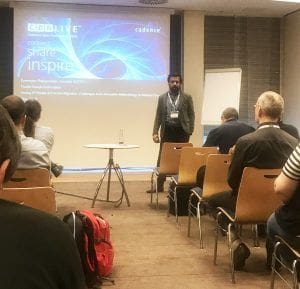
At CDNLive it was particularly gratifying to be able to demonstrate our AMALIA analog migration flow for the first time at a public event. My presentation at the conference – “Analog IP Reuse & Process Migration: Challenges & an Innovative Methodology to Address Them” – illustrated the changes we see in analog design. I believe that human expertise is indispensible, but that some aspects of the analog flow can be sped up and improved using design automation. Migration is a great example – traditionally, a process change has meant a redesign: but as our work with Catena illustrates, there’s plenty we can do in terms of tools and methodologies that support the designer and make the process more efficient.

Analog design reuse – a new approach

TSMC’s Symposium always offers a great opportunity to gauge the pulse of the industry, and this year’s events were no exception. Our CEO Rodger Sykes and Sales Director Jean-Francois Lambert were able to introduce many potential customers to our analog design offering – not only in schematic porting and process migration, but also explaining our ability to facilitate the generation of design variants, and increase performance of existing analog IPs.

Focusing on schematic porting

At the IP-SoC event we were more focused on schematic porting, and once again my presentation was greeted with a lot of interest. We’ve already published a case study on this aspect of the flow, and I was able to provide some detailed facts and figures on the RoI of our new approach to analog design.

Moving into 2019

I’m expecting 2019 to be another exciting year – we’ll have more news on our products and technology developments, expansion in the team, and more significant corporate announcements expected soon.

Thanks for your support and interest in Thalia in 2018, and here’s to a successful coming year!