Ramifications for planning in the face of chip shortages

This is the third and final blog in a short series of posts looking at the chip shortage crisis our industry is facing. Previous posts looked at the political situations both affecting and attempting to tackle the problems, and how the chip makers are ramping up and investing in their own attempts to sensibly fill the supply gaps and maximize on the opportunities as quickly as possible. 

In a previous recent blog, I’ve set out some thoughts on the realities and impacts of chip shortages on the evolving connected car market.  

S&P are scaling back forecasts on car production for 2022, given the chip supply issue affecting the industry. Automotive industry impact: ‘Toyota and Nissan, have scaled back production and others such as BMW, Ford and Volvo have removed certain features from some cars to enable them to continue production.’ 

In the mobile phone markets, Samsung and Apple have been using their might to maintain their own supplies…but other OEMs have been left struggling
“low-end OEMs…struggled the most to adapt with chip foundries expected to take “years” to spool up to demand.” https://www.androidpolice.com/apple-and-samsungs-smartphone-businesses-are-surviving-the-global-chip-shortage-in-ways-only-they-can/ 

In the face of chip shortages and times of geopolitical uncertainty, shortages will continue in the short to mid-term at least, so OEMs looking to remain competitive will need to continually assess their options and consider moving or duplicating (second-sourcing) designs to secure capacity from more than one manufacturing partner. 

Some Tier 2 fabs are positioned ready to seize the opportunities in these times of uncertainty – they can offer attractive costs and potentially be more responsive and adaptable to customer needs. 

Migrating IP to other fabs, design nodes or process technologies can be complex and, itself, time-consuming (hence competitively prohibitive) unless it’s done with the right tools. That is where we at Thalia can help. For 2022 and possibly into next year we need to help our customers reduce their costs in IP migration through innovative IP reuse, and help to maintain their competitive edge. 

Diversification and investments

The second in our series of blogs looking at pressures on the industry of the chip shortage discusses what we see happening in the chip manufacturing (wafer fabs) industry, in particular. This is an industry traditionally dominated by a small number of players and the price of entry is huge – hence, a bit like turning a container ship, these giants take time to move and the costs of expansion are significant. 

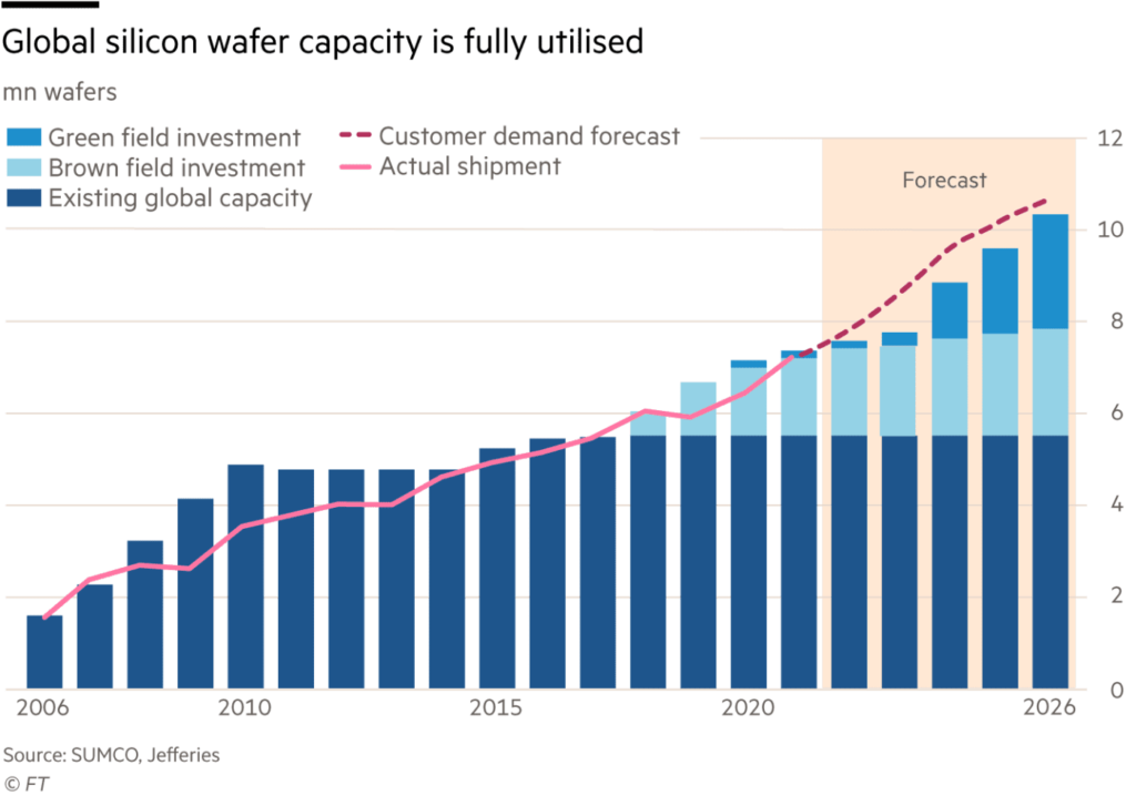
At advanced process nodes (used for mobile devices such as advanced smartphones, tablets), TSMC is responsible for an estimated 92% of global production. Across the board, TSMC still supplies a quarter of the world’s supply of chips (24%) – and its capacity is fully utilised and it continues to expand its facilities: particularly important that this expansion is happening overseas given the geopolitical risks mentioned in the previous blog.  

TSMC is being bullish and believes the demand is a long term upward trend and is even committing $100Bn in investments to expand its own capacity and research facilities.  

But it’s clear that given the geopolitical risk we discussed in the previous blog, TSMC sees the need for its future facilities to be more globally diversified. The technology industry is nervous about the impact on the #1 supplier with tensions once again growing between China and Taiwan. One active TSMC strategy is building the fab in Phoenix, Arizona:  

https://www.cnbc.com/2021/10/16/tsmc-taiwanese-chipmaker-ramping-production-to-end-chip-shortage.html 

The final blog in the short series on ‘chip shortages’ will look at the impact on planning decisions and the measures companies need to take to maintain profitability in the face of time-to-market pressures and a shift in the chip supply chain. 

Geopolitics and global chip shortages

This blog is the first in a series of three snapshot articles on the effects of chip shortage on the industry: What impacts is it having? What changes are taking place in the industry, or even in politics, in attempts to guarantee supplies and ring-fence national or regional supplies? And finally, once plans are in place for second-sourcing, or alternative manufacturing, how does that affect design decisions, time-to-market and ultimately, profitability? 

Access to chip supplies – hence to the manufacturing of chips – have become a strategic initiative for companies and nations alike. Lockdowns due to Covid-19 has arguably caused a lot of the ‘tailbacks’ seen in the industry. But while it’s been a catalyst, there are other factors at play and it’s making nation-states and regions start to evaluate the strategic importance of their chip supplies. 

The fact is, in spite of problems with supply chain, or businesses affected in various ways due to Covid-19 lockdowns, demand has not dropped off, and shows no signs of scaling back. Quite the opposite. 

In fact, we’ve seen in recent weeks, the risks of global conflict certainly affect supply and demand and can impact the industry in ways we’d never thought of, with the growing crisis in Ukraine set to affect the supply of palladium and scandium – some of the raw materials used in chip manufacturing:  

But more generally, changes in the geopolitical climate are making chip companies consider and reconsider where they source or where they manufacture. US politics can discourage or stop companies from moving their manufacturing to China for example.  

Global Wafers attempting to invest in Siltronic – but ‘stalling’ for what appears to be political reasons. 

The big wafer fabs are rethinking their own strategies to both keep pace with the chip shortage and to fend off geopolitical risks that may affect their own supplies or access to their customers. Some of this is the Tier 1 chip makers extending their manufacturing, both to other parts of the world, or in the same region to simply increase their capacity. 

But it’s not a quick fix: wafer fabs take a lot of money and typically at least three years to build and become operational. 

In Europe, the $43bn EU chips act is targeting European self-sufficiency to raise its game – aiming for 20 percent of the global market by 2030. The act also is also designed to prioritise Europe’s own needs ‘in times of shortages’. 

The second blog in this series will look at how companies are restructuring and where investment decisions are being driven by the risks of global chip shortages and these geopolitics pressures.

Connected car: The growing demands of automotive OEMs and the supply chain

In a recent post on EDA Cafe I talked about industry trends, and highlighted how automotive chip usage has traditionally been small by comparison to consumer electronics – but its market is growing.

As a subset of the car market, connected and autonomous vehicles (CAVs) is a market set to grow exponentially in the next five years. In figures from Allied Market Research, the global connected car market was valued at $63.03 billion in 2019, and is projected to reach $225.16 billion by 2027.

The use of other, traditional in-vehicle system, control and multimedia electronics continue to grow.

But there are both opportunities and threats within connected car.

The number of sensors even in traditional vehicles is growing significantly – from an average of 100 today, to at least doubling for a connected car. Connected cars obviously have a certain volume of sensors, wireless communications, and interface devices for driver, passenger or for maintenance. Move into autonomous, and clearly the need for sensors grows rapidly as does the need for more secure and functionally-safe systems.

These opportunities need to be balanced in the face of the (now very real) global semiconductor shortage. System designers will have to tackle capacity issues at foundries and component shortages at their usual semiconductor OEMs. Manufacturing capacity issues are here today and for the foreseeable future.

In October 2021, Tom Caulfield, CEO of GlobalFoundries was quoted as saying that they have sold all capacity until 2023. TSMC and other fabs are rapidly looking for ways to expand their production – but building new cutting-edge wafer fabs takes time (years, not months).

It’s clear the industry is painfully aware of this capacity crunch and ongoing threats to their supplies. Jaguar Land Rover recently pointed to chip shortages for its £9 million loss in the last three months of 2021. Retaining flexibility in design, choice of manufacturing and agility in working with different mixes of components will be crucially important to the automotive industry in the next 24 months.

Sources below:

https://www.ft.com/content/03377749-1fcb-4504-9959-8ebd7f581b2e

Thalia’s IP reuse platform joins Cadence Connections EDA Program

AMALIA IP reuse platform makes it easier for Cadence users to migrate, improve and optimize existing IP for new technologies and applications

Cologne, 11 October 2021 – Thalia Design Automation, an IP reuse company and expert in the development and deployment of automation solutions for analog and mixed-signal IP reuse, today announced it has joined the Cadence® Connections® EDA Program enabling Cadence customers to benefit from cost and time savings when using the Thalia AMALIA IP reuse platform to migrate to new technologies.

The Cadence Connections program encourages interoperability and open industry standards, collaborating with software suppliers worldwide to enhance the value in using Cadence products. Partners are chosen based on seamless product interoperability with Cadence solutions throughout the design flow.

Thalia’s AMALIA IP reuse platform comprises three key elements that align with Cadence workflow – the Circuit Porting capability, the Design Enabler and the Technology Analyzer.

The combination of the Thalia AMALIA platform and Cadence design solutions presents designers and system developers with a powerful combination of tools to make maximum use and reuse of their valuable analog IP.

AMALIA Circuit Porting improves the return on investment of an IP portfolio, enabling the designer to port designs with confidence of their suitability for new nodes or process technologies. Operating in the familiar Cadence Virtuoso® environment, Circuit Porting makes it possible to transfer even large, complex circuits quickly and easily, eliminating the typical complexities and pitfalls.

Also, part of the AMALIA IP Reuse Platform, Thalia Design Enabler software uses artificial intelligence (AI) and machine learning (ML) to save developers up to 50 percent more time and resources when centering designs after migrating from one technology to another. It quickly identifies the minimum set of devices needed to adjust the design the tool, reducing the number of changes required in layout while improving performance.

The AMALIA Technology Analyzer qualifies IP intended for the migration to a new technology. By comparing base and target technologies, Technology Analyzer enables Thalia IP Reuse platform users to not only select the best technology for the project, but to keep costs under tight control.

“Our platform meets the Cadence Connections program objectives and complements Cadence’s Intelligent System Design solutions and services. Together, we’re offering mutual customers a new methodology to facilitate IP reuse via advanced design migration techniques,” said Sowmyan Rajagopalan, Thalia Design Automation CEO.

To learn more about Thalia’s Technology Analyzer, download the white paper at https://www.thalia-da.com/resources/.

Technology agnostic analog circuit and IP migration

Every time you move your designs onto a new process or technology node, the analog circuits and IP need to be implemented. The fact is, managing the migration of these isn’t always the easiest since, as yet, there is no high-level description – as exists in the digital domain.

There are smart ways to reuse part of the layout and schematics for simple designs. However, for complex SoCs to take full benefit of the integration nodes these simple migrations are not recommended.

If you move foundries, the challenges become even more complex as most of them have their own philosophy on creating the PDKs and coping with the latest challenges of sub-nano technology nodes.

For effective decision-making surrounding a circuit design (or redesign), engineering and business planning needs to be able to easily compare the overall business-case, from the feasibility of the design down to the foundry wafer prices and availability of fab capacity and ultimately, to the price of the final device at specific quantities.

It was this set of challenges, and the need for simplifying designers’ lives, that led us to develop the Amalia Technology Analyzer. In the hands of our customers’ design engineers, this powerful tool gives them the option to compare foundry technologies in the shortest time, and informs their strategic planning: enabling them to decide on the right design options and the optimum commercial fit.

Using Technology Analyzer, design teams select the source and target technologies to estimate the best fit, as shown in Figure 1.

Fig 1

Technology Analyzer enables simulations down to device level, using SmartSpice or Spectre, giving the design teams the necessary insights to compare and qualify practically all existing foundry and technology nodes that might fit that specific design. It also gives the possibility to compare the overall costs of productization across different fabs.

And that last point is fundamental when, as is the case today, fab capacity is under extreme pressure and is booked up by a small number of Tier 1 tech companies. The ability to make fast decisions can be crucial to finalize an implementation and to get your product market quickly – hopefully before it’s even too late to maintain your competitive advantage.

If you are under these pressures and this sounds all-too familiar, get in touch with us here and see how a Thalia AMALIA solution can help your business.

Circuit Porting shouldn’t be a shot in the dark

To stay competitive, migration is essential: supporting smaller (or larger!) process nodes, alternative fabs, or diversify designs without starting from scratch. Non-recurring engineering (NRE) costs can undermine product marketing strategies: making migration or diversification prohibitively expensive and eroding your competitive advantages in the market.

Done correctly, it is possible to benefit from savings of 50 percent in both development times and costs, by intelligently employing a strategy of IP reuse to support opportunities for extending your existing products to newer processes or product variants.

However, migrating large analog or mixed-signal circuits can itself seem time consuming and can expose re-designs to problems that can be costly to resolve:

  • Mapping the circuits is time consuming and it’s easy to make mistakes
  • You need to account for scaling when porting to different process nodes
  • You need to follow all target device parameter restrictions and create a solution to keep device parameters consistent with source designs

Without insights into where there may be problems or where there are room for improvements, designers have no insight into tolerance limits. They won’t find out about these limits until they run into them – and that’s usually too late.

All of this leaves a re-design open to potential issues which could affect design times, impact performance, as well as undermine the potential profitability of the entire process migration.

A circuit porting tool such as AMALIA OA Circuit Porting (for OpenAccess database) from Thalia, provides a familiar Cadence Virtuoso environment to quickly and easily port circuit designs.

Key steps in circuit porting using AMALIA Circuit Porting OA:

  • Mapping file (Device Mapping file generator)
  • Select your designs (easy-to-use GUI)
  • Port automatically
  • Automatically solve issues with target parameter restrictions
  • Compare existing and ported designs, errors are flagged and highlighted for easy identification
  • Verify the resulting design on the new process

 To allow customer engineering teams to focus on developing new innovative solutions, it’s important that the IP reuse tasks such as circuit porting are supported by a strong team – this is as important as the porting tool itself. The Thalia team behind OA Circuit Porting includes experienced tool developers, mathematician, and hands-on system developers – offering customers a complete understanding of how best to port your design.

Main UI of OA Circuit porting:

OA circuit porting toolbar:

Chiplets and IP reuse made easy: Smaller node ASICs are not always the best way forward

Chiplets are a relatively new trend in helping designers of large complex system design to enable a cost-effectively modular approach to designing with costly SoCs. I say relatively because proposals started back in 2016 when DARPA used it as part of its CHIPS (Common Heterogeneous Integration and IP Reuse Strategies) program.

To quote DARPA, “The monolithic nature of state-of-the-art SoCs is not always acceptable for Department of Defense (DoD) or other low-volume applications due to factors such as high initial prototype costs and requirements for alternative material sets.”

If you look at the economics of SoCs it’s easy to understand why chiplets are of increasing interest to a wide range of system designers – not just the likes of DARPA: moving from a 45 nm process to a 16 nm process more than doubles the cost/mm². Migrate again to a 7 nm process and costs / mm² double again – that’s 4x the cost per yielded mm².

Chiplets do sacrifice some space (around 10 percent) for the ‘chiplet architecture’ – i.e. the chip interconnects, but the overall benefits of chiplets on total system costs is substantial.

The fundamental benefits of a chiplet approach are: low cost and easy way to repurpose the design and enable variants, with some die-to-die interconnect, a range of third party chips can be combined into a package. One of the most important contributing factors enabling the chiplet approach to system level design is today’s advanced packaging technologies.

Many of the benefits and how chiplet design works may sound rather familiar because it’s what Thalia Design and others in the IP Reuse industry have been enabling for decades. In fact, we see huge potential in chiplets and, done correctly, a strategy of reusable chiplets will present enormous time and cost savings. Time to market, ease of design / migration to new processes, familiarity with the design…all of the benefits Thalia’s AMALIA (TM) IP Reuse platform enables.

When approaching the chiplet design, you can create a portfolio of IP for dedicated functions, even before committing the design to silicon. This makes your chiplet design both technology-agnostic and fab-agnostic.

Thalia’s AMALIA Circuit and IP reuse platform gives you that flexibility. Thalia methodology ports your existing chiplets to new technology nodes or fabs in the shortest possible time.

Commercial considerations can be taken into account during the implementation. For example, if the final solution needs to use a specific foundry, for strategical reasons, the chiplets can be quickly and easily ported to that specific foundry and even technology node.

That raises the levels of flexibility in complex system-level implementations and also gives customers the maximum flexibility in defining their system-in-package solution.

The AMALIA platform only needs the chiplet source technology database and PDK, plus the target technology PDK. AMALIA can also help to create a complete chiplet portfolio. Thalia IP reuse suite of products can handle the complete design, reuse or migration of the chiplet in practically every fab or technology node.

Thalia’s partner network also provides the productization of chiplets in specific foundries, down to 7nm technology nodes.

If you are planning your own chiplet strategy, get in touch with us to find out how AMALIA platform can help to further simplify the IP reuse.

AI: when is it ‘really’ intelligent?

Artificial Intelligence is quite obviously a buzzword which attracts significant marketing hype – that has been the case for a decade at least. There are countless number of high-profile examples where AI is used to simply describe an automated (usually software-enabled) routine. Good examples of this can be seen in Facebook’s use of AI: filters that simply track and flag keywords, or images, that break a set of human-defined rules. The fact of the large number of false positives they ‘capture’ demonstrates that, while these programs may be artificial, they’re not always intelligent as we humans would define it. They are, more often than not, just forms of computational automation.

Don’t get me wrong, computational automation can be beneficial, it can speed things up and save significant time, hence money. But it does not add skills, nor does it bring added, intelligent value to a design team – which is what we’re trying to do for our customers. Given the wide and potentially misleading use of the term, there is no doubt that when we chose to use AI to refer to the capabilities of our AMALIA Design Enabler we really had to pause and check we were being honest with ourselves, and with our customers.

AMALIA Design Enabler passes the acid test. We threw problems at the system, asking it to find solutions to problems – looking for answers we didn’t know existed. In the video, you can see a perfect example of its application and the benefits of a truly-AI solution for supporting design problems: helping the designer to compare and assess alternative components to resolve a technical issue with the system. In this case, during a process migration, a very low current voltage regulator was taking far too long to achieve a zero temperature coefficient state… to compare the options and find a solution just in the small circuit in question could have taken the design team several weeks.

By entering the requirements into AMALIA Design Enabler, along with the options available, the Design Enabler AI algorithm was able to find its own way to the answer in relatively few steps and a very short amount of time: reaching the answer in just 40 steps, in spite of there being thousands of potential variables.

The reason we’re confident in calling the Design Enabler true-AI, is exactly that: the system is learning as it goes, changing direction based on initial findings and zeroing-in on the correct solution: it is not simply observing, calculating, and running every possible scenario before ‘happening’ upon the correct answer by brute force and computational power.

So, AI is dead. Long live AI! We believe that true-AI does have a place in design automation. Selecting the appropriate components and enabling appropriate IP reuse in process migration can be a complex, time-consuming task – but when it’s done well, it significantly improves design profitability and system performance.

Thalia’s AMALIA Technology Analyzer de-risks Analog IP reuse for major IP houses and IC manufacturers

Comparing process technologies before commencing migration enables IP houses and IC manufacturers to establish the business case for targeted portfolio expansion 

Cwmbran, UK, May 18th, 2021 Thalia Design Automation, an IP reuse company and experts in the development and deployment of automation solutions for Analog & Mixed Signal IP Reuse, today announced further upgrades and enhancements to its Technology Analyzer.


This latest iteration of the platform means Thalia can better support IP houses to assess process technologies parameters that impact on their portfolio expansion. Much of the effort involved in migrating an IP from one technology to another is associated with qualifying the IP in the target technology. If a block fails to meet the requirements in the target technology, the IP/IC’s performance would be sub-optimal.


The Technology Analyzer is part of a suite of solutions offered by Thalia and sits in parallel with its AMALIA IP reuse platform. Combining the design expertise, proprietary advanced methodologies and AI embedded in the AMALIA platform with this latest upgrade to the analyzer tool, early assessments of the validity of IP migrations is easier than ever.


“The Technology Analyzer has always been an integral part of our unique offering to clients, and this latest iteration of the powerful tool is the next step in its evolution,” said Sowmyan Rajagopalan, Thalia Design Automation CTO. “Understanding the impact and influence of technical parameters on the migration process will always be vital to successful migrations. We’re delighted with this latest upgrade that enables business case and commercial modelling to be undertaking for our clients to assess the value in a migration before committing resource.”


Discussing a recent engagement with this identification of differences, Frédéric Masson, Director of Power Management Solutions at Dolphin Design, said: “We needed to migrate an existing Analog IP to a 22nm process with a tight deadline and a set of key characteristics that had to be addressed. Thalia deployed its Technology Analyzer to assess the device characteristics in the target technology and rapidly determine the best porting strategy to meet critical performances. Combined with Thalia’s AMALIA IP reuse platform, we have been able to anticipate technical issues in the porting and ease the migration within a shorter development cycle.”


Thalia is continuing to evolve and develop its suite of tools and platforms to deliver the best possible results for IP houses and IC manufacturers while harnessing the power of AI alongside its expert team of design engineers and advanced methodologies.


Download our new white paper to understand more about Thalia’s Technology Analyzer here: https://www.thalia-da.com/resources/


About Thalia Design Automation

Thalia Design Automation, an IP reuse company, is expert in targeted automation for analog and mixed signal design and IP reuse. Thalia’s AMALIA IP re-use platform migrates, improves and optimizes existing IP for new technologies and applications. Our customers – IP houses, Tier 1 players and foundries – can leverage the platform to re-use and diversify their product ranges quickly and cost effectively to meet ever-changing market demands. Our highly skilled design engineers and advanced methodologies combine with AMALIA’s AI algorithms to deliver outstanding efficiencies in the analysis, design and verification stages of IP re-use. The result is a reduction in development time of up to 50%, allowing our clients to react quicker and more effectively to changing market demands.

For more information visit www.thalia-da.com